History
The bipolar point-contact transistor was invented in December 1947 at the Bell Telephone Laboratories by John Bardeen and Walter Brattain under the direction of William Shockley. The junction version known as the bipolar junction transistor, invented by Shockley in 1948, enjoyed three decades as the device of choice in the design of discrete and integrated circuits. Nowadays, the use of the BJT has declined in favour of CMOS technology in the design of digital integrated circuits.Germanium transistors
The germanium transistor was more common in the 1950s and 1960s, and while it exhibits a lower "cut off" voltage, typically around 0.2 V, making it more suitable for some applications, it also has a greater tendency to exhibit thermal runaway.Early manufacturing techniques
Various methods of manufacturing bipolar junction transistors were developed[8].- Point-contact transistor – first type to demonstrate transistor action, limited commercial use due to high cost and noise.
- Grown junction transistor – first type of bipolar junction transistor made[9]. Invented by William Shockley at Bell Labs. Invented on June 23, 1948[10]. Patent filed on June 26, 1948.
- Alloy junction transistor – emitter and collector alloy beads fused to base. Developed at General Electric and RCA[11] in 1951.
- Micro alloy transistor – high speed type of alloy junction transistor. Developed at Philco[12].
- Micro alloy diffused transistor – high speed type of alloy junction transistor. Developed at Philco.
- Post alloy diffused transistor – high speed type of alloy junction transistor. Developed at Philips.
- Tetrode transistor – high speed variant of grown junction transistor[13] or alloy junction transistor[14] with two connections to base.
- Surface barrier transistor – high speed metal barrier junction transistor. Developed at Philco[15] in 1953[16].
- Drift-field transistor – high speed bipolar junction transistor. Invented by Herbert Kroemer[17][18] at the Central Bureau of Telecommunications Technology of the German Postal Service, in 1953.
- Diffusion transistor – modern type bipolar junction transistor. Prototypes[19] developed at Bell Labs in 1954.
- Diffused base transistor – first implementation of diffusion transistor.
- Mesa transistor – Developed at Texas Instruments in 1957.
- Planar transistor – the bipolar junction transistor that made mass produced monolithic integrated circuits possible. Developed by Dr. Jean Hoerni[20] at Fairchild in 1959.
- Epitaxial transistor – a bipolar junction transistor made using vapor phase deposition. See epitaxy. Allows very precise control of doping levels and gradients.
Theory and modeling
In the discussion below, focus is on the NPN bipolar transistor. In the NPN transistor in what is called active mode the base-emitter voltage VBE and collector-base voltage VCB are positive, forward biasing the emitter-base junction and reverse-biasing the collector-base junction. In active mode of operation, electrons are injected from the forward biased n-type emitter region into the p-type base where they diffuse to the reverse biased n-type collector and are swept away by the electric field in the reverse biased collector-base junction. For a figure describing forward and reverse bias, see the end of the article semiconductor diodes.Ebers–Moll model
The DC emitter and collector currents in active mode are well modeled by an approximation to the Ebers–Moll model:


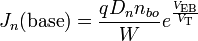
- VT is the thermal voltage kT / q (approximately 26 mV at 300 K ≈ room temperature).
- IE is the emitter current
- IC is the collector current
- αT is the common base forward short circuit current gain (0.98 to 0.998)
- IES is the reverse saturation current of the base–emitter diode (on the order of 10−15 to 10−12 amperes)
- VBE is the base–emitter voltage
- Dn is the diffusion constant for electrons in the p-type base
- W is the base width
The unapproximated Ebers–Moll equations used to describe the three currents in any operating region are given below. These equations are based on the transport model for a bipolar junction transistor.[21]
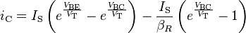


- iC is the collector current
- iB is the base current
- iE is the emitter current
- βF is the forward common emitter current gain (20 to 500)
- βR is the reverse common emitter current gain (0 to 20)
- IS is the reverse saturation current (on the order of 10−15 to 10−12 amperes)
- VT is the thermal voltage (approximately 26 mV at 300 K ≈ room temperature).
- VBE is the base–emitter voltage
- VBC is the base–collector voltage
Base-width modulation
Main article: Early Effect
As the applied collector–base voltage (VBC) varies, the collector–base depletion region varies in size. An increase in the collector–base voltage, for example, causes a greater reverse bias across the collector–base junction, increasing the collector–base depletion region width, and decreasing the width of the base. This variation in base width often is called the "Early effect" after its discoverer James M. Early.Narrowing of the base width has two consequences:
- There is a lesser chance for recombination within the "smaller" base region.
- The charge gradient is increased across the base, and consequently, the current of minority carriers injected across the emitter junction increases.

In the forward-active region, the Early effect modifies the collector current (iC) and the forward common emitter current gain (βF) as given by:[citation needed]


- VCB is the collector–base voltage
- VA is the Early voltage (15 V to 150 V)
- βF0 is forward common-emitter current gain when VCB = 0 V
- ro is the output impedance
- IC is the collector curren
Ricardo A. Monroy B. C.I. 17646658
EES
No hay comentarios:
Publicar un comentario